

Photolithography (photoresist) material
In the recent rapid progress of manufacturing ultra-fine
semiconductors and flat panels, the processes are
increasingly diversified. The ability to rapidly develop
suitable materials is needed. We are developing a
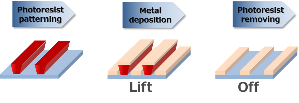
characteristic photoresists (photosensitive materials) for
lift-off processing. Lift-off processing has the advantage
of eliminating a metal etching process for wiring, thus
contributing to shortening the process time and reducing the
amount of material used. We also offer consultation on
material development to meet our customers’ individual needs
and detailed requirements. We look forward to hearing from
you through the contact form below.
View
Product Catalog.
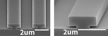
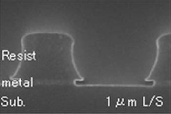
Under Layer Material for Bi-layer Lift-off Processing―BLX Series
- Ideal for a variety of over layer resist applications free of inter-mixing
- Various film thicknesses can be designed for over and under layers
- The amount of side etching can be adjusted as desired depending on the process conditions
- Good easy to be cleaned up
- Possible to replace existing material
- Application examples: Compound semiconductors, optical devices, RF devices, and difficult to etching materials
Film thickness adjustment
Adjustments of the amount of side etching in ultra-thin
films
Inquiries
For product related inquiries, please fill in the form.

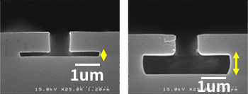
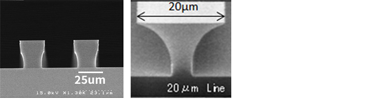
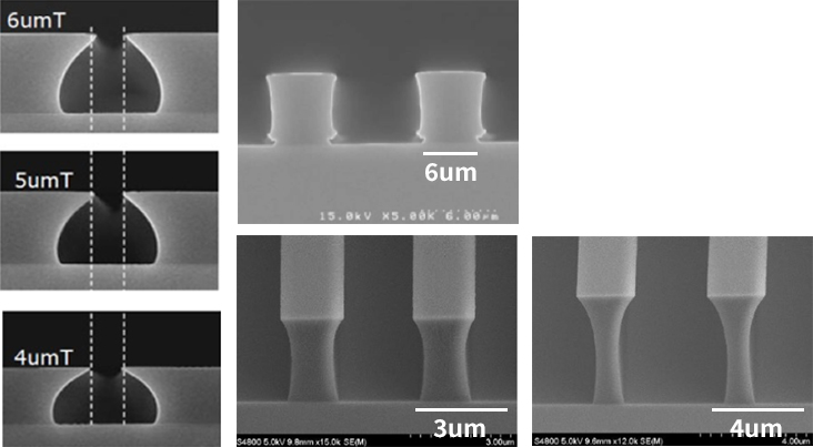
Photoresist for Single Layer Lift-off Processing: NPR9700 Series
- Positive Resist for Lift-off Processing
- Exposure wavelength range: g-line to i-line (broadband compatible)
- Easy to form a anti-taper shape with no special process.
- Good easy to be cleaned up
- We can offer the film thickness, line width, shape, etc., to meet your needs.
- Application examples: Compound semiconductors, optical devices, RF devices, and difficult to etching materials
Inquiries
For product related inquiries, please fill in the form.
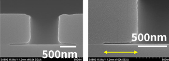
Photoresist for UV Laser Direct Writing―GRX-M Series
-
Ensuring coating performance with a spin coater and
capillary coater used.
Good coating performance on large glass substrates. - Exposure wavelength range: g-line to i-line (broadband compatible) Suitable for laser writing.
- Organic and inorganic alkaline development possible.
- The optimized material composition has improved the in-plane uniformity of line widths on large glass substrates during direct laser writing.
- Improved metal etching performance by optimizing the pattern profile
- Excellent adhesion on the substrate with low side etching.
- Good easy to be cleaned up
- Application examples: Liquid crystal displays and photomask blanks
We are also developing various special resists and photosensitive insulating films. Please feel free to contact us.
Inquiries
For product related inquiries, please fill in the form.
Product Catalog
Photolithography (photoresist) material(331KB)
The application examples shown on this website and in catalogs
do not guarantee the application results of our products.
Please evaluate their suitability for your application,
purpose of use, and conditions when using our products.
Furthermore, we do not guarantee that the application examples
presented here are free from infringing any intellectual
property rights.